
On September 14 the population-wide rollout of the token began. I collected mine two days later for use while running because they’re much easier to carry and to waterproof than a phone is. Today I finally got around to opening it up.
Per GovTech’s announcement in August, the company who made the initial batch of tokens that we examined at the teardown session (PCI) was also one of the successful bidders for the larger project. My token is all but identical to those that we examined, so I assume that it’s one of those made by PCI. The one material change that I’ve identified so far is a bit of a mystery though: an IC has been removed!
Clock side
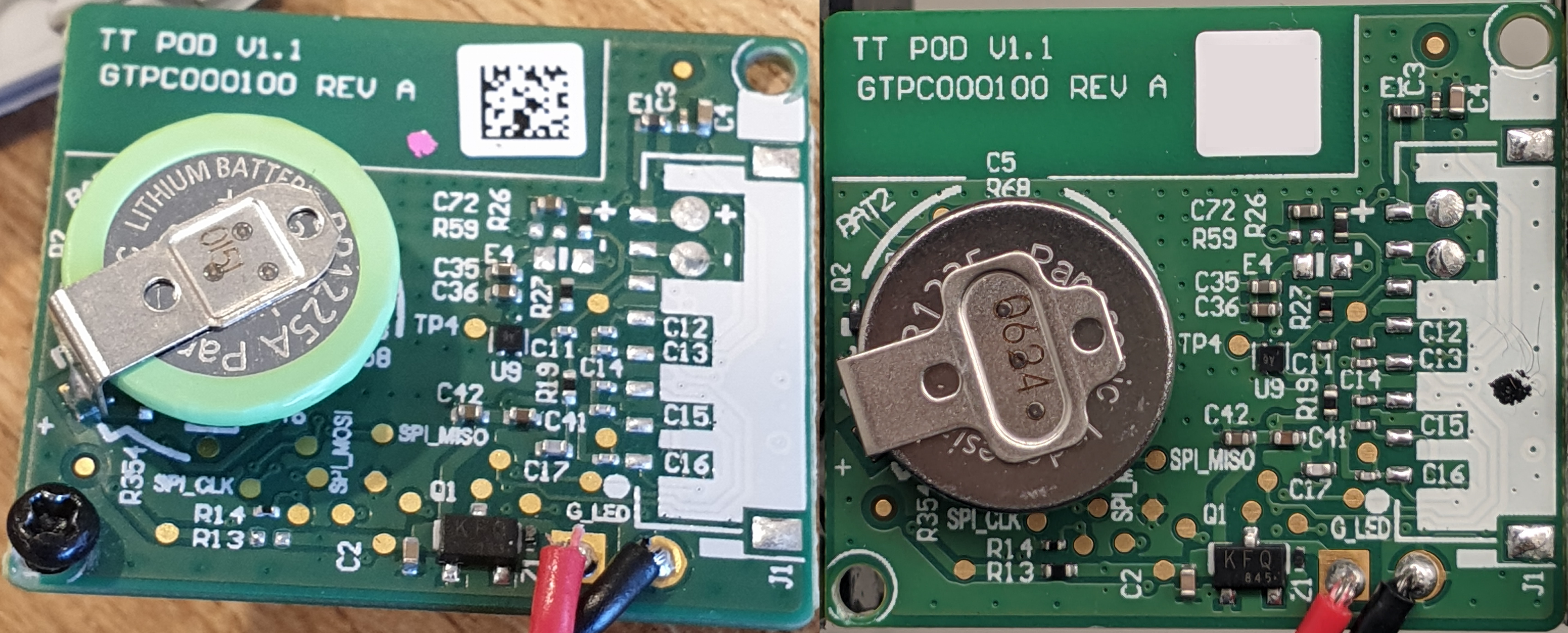
On the left is the token that I examined during the teardown session in June; on the right is the one that I collected for personal use a few weeks ago. The boards would appear to be identical, right down to their being “REV A”. The sticker to the right of REV A does differ between boards and appears to contain 196 bits of information, which suggests a unique identifier, so I’ve blanked it for my personal one.
The built-in coin cell is BAT2 and is presumably used to power a real-time clock. This is separate from the much larger, removable coin cell that’s used to power the entire token. More below.
U9 (to the right of the battery) is something of a mystery at present. It’s a 4-pin device which appears to be labelled A6 with 6 underlined and A “overlined” (is there a better word for this?). Some study of the copper traces and vias on the boards is going to be required to infer its place in the system. The proximity to a test point (TP4) is interesting.
Q1 (labelled KFQ 845, near the bottom) would appear to be a voltage regulator, although I’ve not been able to identify it. Z1 immediately beside it is presumably a Zener diode to protect the system against excessive voltage from installing the wrong battery or similar, both because of its being in parallel with the main coin cell and the regulator, and the unusual name (Z is not a standard class designator).
Clock area
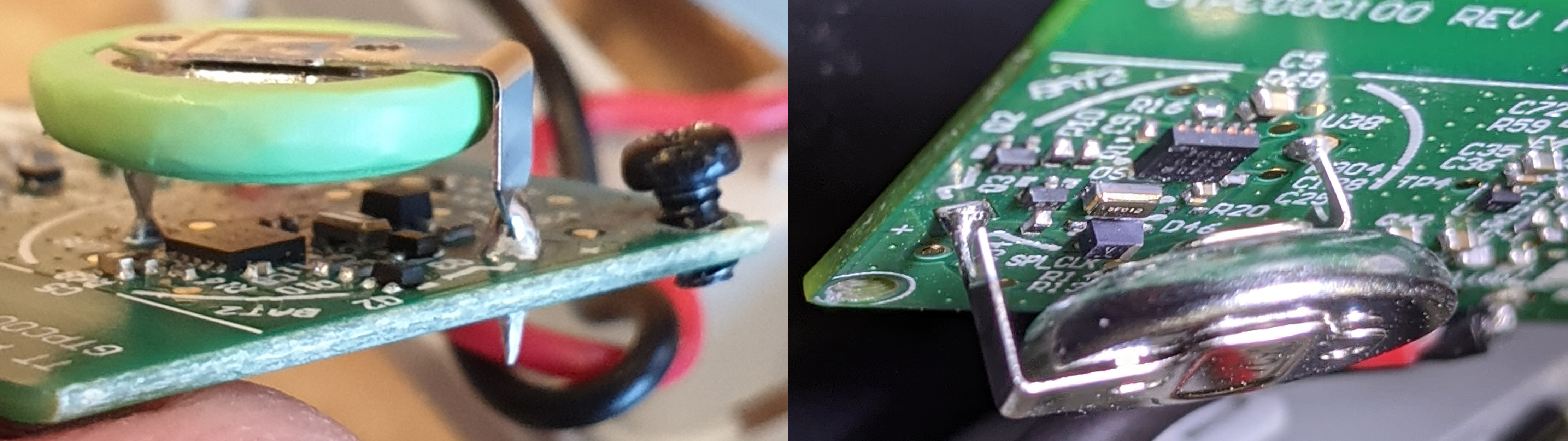
The way this is laid out happens to make tampering with the clock chip difficult in that you’d need to remove the coin cell first, at which point the clock would stop. (Yes, you could power it separately, etc., but it would be more difficult.) Perhaps it’s just about putting all of the clock-related stuff in one part of the board.
There’s not much here:
- U38 is labelled “363A” “0123” “e02 1”. My best guess is an NXP PCF85363A however it appears to be a little smaller than is stated in the spec sheet (2.6mm specified, closer to 2.3mm measured).
- An oscillator (the metallic tin to the right of/below the IC).
- A pair of transistors.
- A surprisingly tall diode in the background.
Antenna side
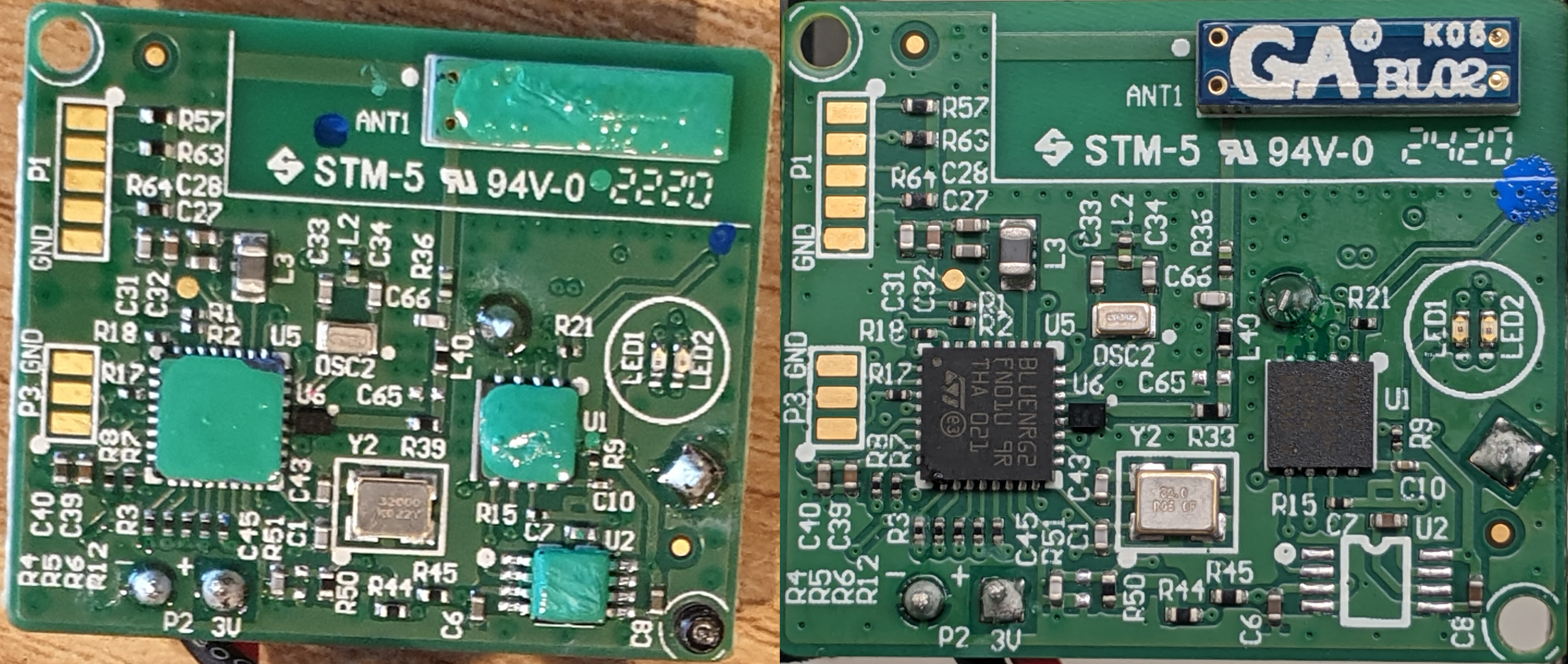
The masking of the part numbers at the June session is the rather obvious green paint covering the antenna and the larger chips.
- ANT1 at the top right appears to be a Green Antenna GA123416BL02 CUB 2.4GHz SMD Antenna.
- U1 near the right centre is the storage device for logging contacts, a Macronix MX25R6435F 64Mb flash memory. (The text is so faint that I wasn’t able to get a readable photograph of it.)
- U2 at the bottom right is …missing!
- U5 near the bottom left is a combined SoC and radio, an ST BlueNRG-2.
- U6 immediately to the right of U5 appears to be an ST BALF-NRG-02D3 balun or conjugate match, to couple U5 to the antenna.
It’s worth noting that the BlueNRG-1 and BlueNRG-2 are pin-compatible (the latter can be slightly more efficient during sleep), meaning that we can’t say for certain which IC was present at the teardown session, but given the layout of the surrounding power supply components (L3, C27, C28), oscillator components (OSC2, C33, C34, L2) (OSC1, C1, C43), and antenna match (U6, R33, C65 (missing), L40, C66, R36) — all of which appear to be according to the reference design from the ST documentation — we can reasonably rule out any materially different IC. This has an important consequence: I had assumed a separate SoC and radio ICs, but the BlueNRG ICs combine both of these functions onto a single IC, which begs the question: why were there three large ICs at the teardown session? At present, I have no idea:
- It’s clearly not essential for the token’s function or it couldn’t have been removed.
- The inclusion of additional-cost components during development and removal during mass production is not unheard of, but it had to be doing something useful or it would not have been present.
- U2 has no access to the antenna, even if it did a 2.4GHz antenna would not be useful for GPS or phone, and as previously noted the power source isn’t adequate for these functions anyway.
- There’s no hole in the board beneath U2, which would have been required for most MEMS microphones.
- A MEMS accelerometer to have it turn the receiver on for longer or more frequently when the user moves?
- A crypto-processor for more energy-costly methods of identification or DoS-control?
- Offboard storage of firmware to simplify development?
That’s all I have for today. More soon!